Solid State Drive Primer # 2 - SLC, MLC and TLC NAND Flash
![]() This article builds on the earlier Basic NAND Flash Cell article, by showing the advances in technology from the original SLC to MLC, and TLC NAND Cells.
This article builds on the earlier Basic NAND Flash Cell article, by showing the advances in technology from the original SLC to MLC, and TLC NAND Cells.
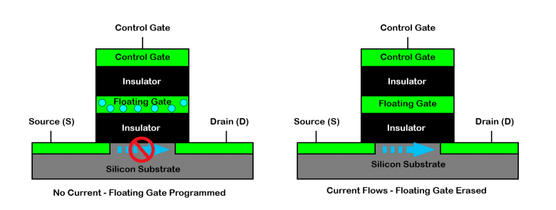
For a simple review of the Basic NAND Cell, charges are either stored or not stored on a floating gate which is sandwiched between two layers of oxide which act as an insulator.

If current flow is detected, it indicates the floating gate does not have a charge and is erased, representing a binary 1. See diagram above right.
How MLC and TLC store more than one bit per cell
The example above shows a SLC (Single Level Cell) NAND Cell. When any current is detected between the source and drain it can be concluded the cell is programmed. Since only two states, programmed or erased, are needed to represent one bit, that’s all that is needed.
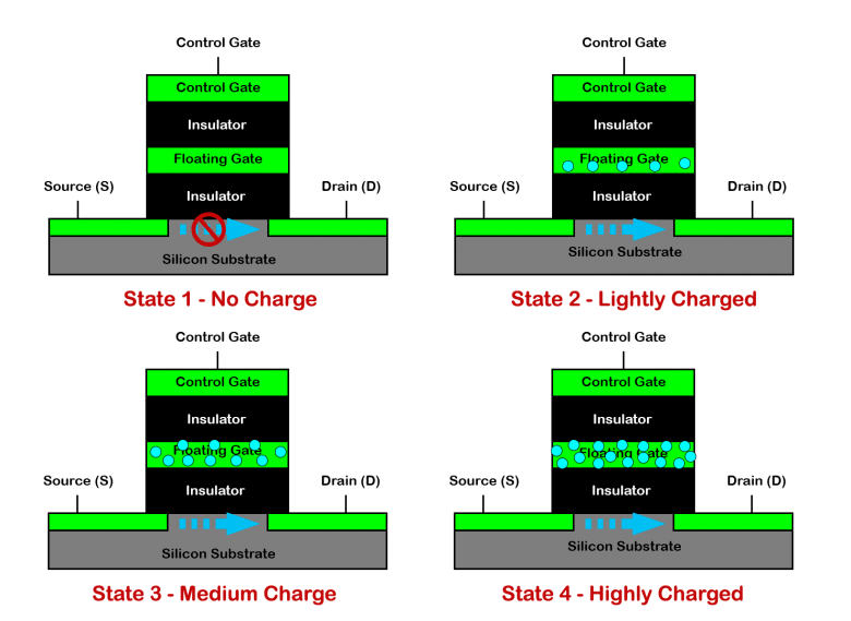
With MLC (Multi Level Cell) NAND, there is a need to store two bits of data, which requires 4 distinct states. In order to accomplish this, the MLC NAND cell must be able to apply charge to the floating gate at four different levels and later be able to detect which of the four levels is set.
The diagram below represents the additional electrons in blue on the floating gate which must be set to precise levels so they can later be read accurately. This makes MLC more challenging and slower to write than their SLC NAND counterpart.

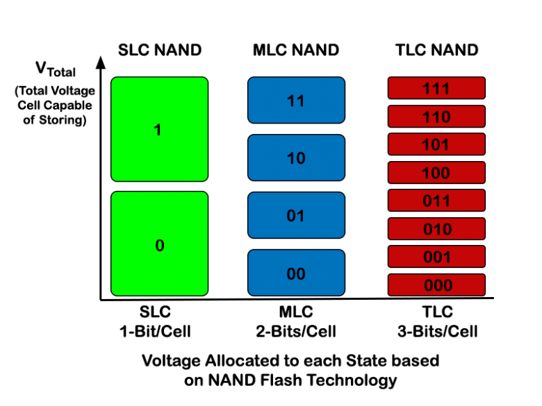
Voltage Level in SLC, MLC and TLC NAND Cells:
The maximum voltage in each cell is about the same. So SLC cells have plenty of guard band between their states. Because of this, SLC NAND is able to withstand temperature extremes and other adverse effects much better than MLC or TLC NAND.

If you would like to discuss further, please contact us.


